|
|
Two Layer DesignFour Layer Design
Ignition and Injector Driver BoardsThe Current 4-Layer Board
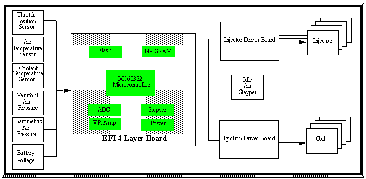
This page describes the current version of the Electronic Fuel Injection (EFI) control board under development by Bruce Bowling and Al Grippo. This board, denoted as the "4-layer EFI" board (mainly because the circuit board consists of 4 layers: one power, one ground, and two signal), is the current incarnation of the efi332 project. This board consists of the following sections:
Embedded ControllerThe CPU section is based on a Motorola 68332 microcontroller, and is similar to the CPU board section of the EFI332 board (designed by Rod Baram). This microntroller contains on-board analog-to-digital converters and a sophisticated Time Processor Unit. The CPU section uses flash and non-volatile SRAM memory devices for program and data. This section is the heart of the 4-layer EFI board. Sensor InputThe Sensor section consists of the analog and digital circuitry
required to condition the various input measurement devices, which include: Fuel Injector OutputThis section provides the line drivers for an off-board fuel injector power board. The timing for the injection pulses are generated by the TPU section of the CPU. There are eight separate drive lines which can serve one or more injectors each. Spark Ignition OutputThis section provides the drive circuitry to trigger an off-board ignition driver board. The calculations of trigger events and dwell is performed by the TPU in the CPU section. There are two signals associated with this section - one which is the trigger for the ignition event, and another which serves as a sync reset which denotes cylinder number one (this is used by the ignition driver board). Power SupplyThe power supply section provides the required voltage regulation for the semiconductor devices. In addition, this section provides protection from abberations on the vehicle's electrical system, including noise spikes, polarity reversals, and brownouts, as well as filtering noise which are always present in an operating vehicle environment.
Back to TopSchematic Diagrams
Board Layout Scans
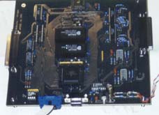
Actual Board Scans
Back to TopCommon Assembly QuestionsScavenged from posts to the list: Q1. The PDF schematics don't show a pullup on the RESET line that I can see, but it is there on the hand drawn schematics from Bruce/Al. The value is very hard to read. I guessed and put a 10k and it seems to work fine. Does value really matter? This one is particularly important since without it, the BDM won't even work correctly. A1) 10k will work fine. Q2) In my parts kit and on Bruces parts list, there is a Reset supervisor. Where does this go on the board? It's not on the PDF schematic or the hand drawn one that I can see. A2) It is on the hand-drawn picture, under the "BDM/Serial Comminications" link: http://www.diy-efi.org/~bbowling/bdmser.jpg Its the MCP120-475DI part. Q3) There a few components missing on the PDF schematic which are on the hand drawn schematic. The are two fairly important caps which go underneath the processor for the PLL. These caps can make or break a board. Trust me - we have had problems with Motorola PLLs that even Motorola didn't even have a straight up answer for. A3) Use the hand-drawn pictures for assembly. And these caps *are* show-stoppers indeed! Q4) A while back Bruce said "Be sure to put the rubber spacer over the CPU socket BEFORE you solder the socket to the board. If you fail to do this, then throw the board in the trash, because it is next to impossible to remove the socket." when it came to making the 4 layer board. A4) This plastic piece, which is only pushed halfway on the socket pins, is used to keep the pins from being bent during shipping, AND is used as an insulator for the socket - just push the plastic piece flush with the socket. You can see how the pins bend all which ways under the socket and this piece keeps this insulated from the board. Since there is a soldermask on these boards if one forgets the spacer the board *may* still work, but it will be by luck only. Q5) Does the flash (am29f010) have to be 70 ns or could I use 90 ns parts ?? I have lookt though the 332 datasheet without finding an answer (I have some 90 ns laying around I would like to use) A5) 90ns will work, but you will have to increase wait-states. Q6) Charles' BDM board notes say that pin 1 of the small connector is on the left when facing the connector. It appears to be the same on the 4-layer board, i.e on the left when facing the connector. Is this correct? A6) Al *always* uses a square pad to indicate pin 1 on sockets, plugs, etc, and the hand drawings also will always show a square pad for pin #1. Q7) the diy-efi site is missing the files octser.jpg and step.jpg. I was able to find step.jpg at Al Grippo's page but not octser.jpg either. Can someone make these available please? The assembly of the output section should be simple but is not obvious without these diagrams. A7) First, there was a bug in the 4-layer page in my HTML (Bruce left off a ") which made some of the links not appear, specifically the octal serial and buffer scans. This is fixed now. Also, the octal serial page also shows the OLD stepper motor chip. Remember that the stepper motor chip was replaced with a newer chip, and this layout scan is on a separate link page (the "Stepper Motor New" link). The WWW site has a warning about this. Also, the WWW page is now at http://www.diy-efi.org/~bbowling - Bruce updated this page only. Do not use the old sura1.jlab.org link anymore. Q8) What is the function and normal positions of the DIP switch block? A8) Only one switch contact (the far left one) is used, which is used by the software to see if either a laptop (running the mainpc.exe monitor program) or if a LCD/button box (used as a passenger compartment monitor - this device is a 2x20 line LCD and a serial backpack encased in a small box) is connected to the serial port. Q9) From the schematic, the stepper chip has a 3 pin header/jumper nearby. My parts kit did not include any headers or jumpers. Was this an omission? If it is supposed to be there what is its function and what is the normal position of the jumper? A9) The jumpers are used for different operating modes of the stepper motor chip (like PWM current limiting control, etc). The position of the jumper is really dependent on your end IAC motor. One thing I strongly suggest is to download the datasheet for the stepper motor chip - the functions of the jumpers will become clear. There are also jjumper blocks around the LM1815 chips to allow either VR or digital signals. Once again, look at the datasheet for the different operating modes. Q10) Where do the 1 ohm, 1 watt resistors go? I have not come across them in the sketches or schematics. A10) Around the new stepper motor chip, which you will see on the now-fixed WWW site. This value affects the operation of the current-limit, and you may want to adjust its value - see the datasheet to understand this better.
|
|
Thanks to Bowling & Grippo for their financial support of this site!